


Home > Research > Pickup > takayoshi_yokoya
Using synchrotron radiation to obtain a more detailed picture of the electron:Tackling the puzzle of the superconducting diamond
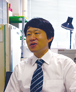
Takayoshi Yokoya
Professor of Physics
After obtaining his Ph.D. in physics from the Tohoku University Graduate School and Faculty of Science, he performed his post-doctorate work at the same school as a recipient of a Research Fellowship for Young Scientists from the Japan Society for the Promotion of Science. After serving as a Research Associate at the Institute for Solid State Physics, University of Tokyo, he worked as team leader and chief researcher of the Soft X-Ray Team within the Research & Utilization Division of the Japan Synchrotron Radiation Research Institute (JASRI). Since 2005, he has served as a full Professor at Okayama University, at the Research Institute for Interdisciplinary Science (RIIS) and the Research Laboratory for Surface Science (RLSS).
Professor Yokoya's research lab uses synchrotron radiation to investigate the behavior of electrons within materials, with the aim of understanding various properties displayed by materials.
Professor Yokoya explains his work as follows.
"Properties shown by materials, such as metals, semiconductors, and superconductors, are determined by the properties of the electrons within each individual substance. Photoemission spectroscopy enables the capture of the complete electron energy distribution within a material. The SPring-8 large-scale synchrotron radiation facility creates the world's highest performance light (X-rays), which we use to achieve our goal of being the first in the world to ascertain the phenomena shown by new materials."
The superconducting diamond
Diamonds are made from carbon and are therefore similar to the carbon-based fullerenes and carbon nanotubes, serving as core materials in nanotechnologies that industries are also interested in. While diamonds are known as representative precious stones, they are also valuable in industrial uses as their hardness is utilized in cutting tools and abrasives. Recently there has been hope that diamonds can also be used as materials for electronic devices, as the addition of impurities in diamonds provides electrical conductivity characteristics.
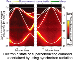
In 2004, a Russian research group reported that with boron doping, diamonds can also become superconductors. Professor Yokoya's group was the first in the world to use angle-resolved photoemission spectroscopy (ARPES)*1 to study the properties of superconductivity in boron-doped diamonds. This group became the first worldwide to elucidate the electron structure responsible for this electrical conductivity. They found that holes in the band structure originating from the diamond play a major role in this conductivity. This discovery will likely contribute to the development of future diamond devices that utilize superconductivity.
In the field of condensed matter physics, there have been many pioneering discoveries, such as the superconducting diamond, high-temperature superconductivity, and other exciting phenomena. Professor Yokoya and his team have been using synchrotron radiation methods to clarify the electronic structure within a variety of these materials.
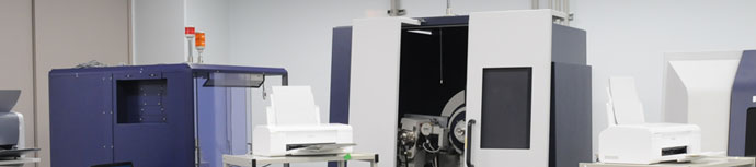
"To understand the various characteristics displayed by superconducting and other materials, one requires a detailed understanding of the internal electronic structure of these materials. Photoelectron spectroscopy is a method suited for such observations. However, this was impossible with the insufficient resolution capabilities of conventional devices. The only way we would be able to see what others could not know was to construct the world's highest performance photoelectron spectrometer."
Professor Yokoya continues, displaying his enthusiasm.
"I like to penetrate deeply into whatever I find interesting. In our work, we observe things that have never been possible to see before, and using a machine we built ourselves we can understand phenomena displayed by new materials. This is truly exciting."
Research Laboratory for Surface Science
Dr. Yokoya's lab is located in the Research Laboratory for Surface Science (RLSS) attached to Okayama University. The importance of surfaces and interfaces has grown with the inclusion of industry in this field. The RLSS is the first such research institute for the study of surface science established in Japan, thanks to the vision of Okayama University.
"At the surfaces and interfaces that connect one material with another, the occurring phenomena are different from those occurring within the materials themselves. In our daily lives, we often encounter such surface phenomena, such as adhesion and adsorption. In the electronic devices of the near future, it will be necessary to control the contact surfaces between semiconductors and a variety of new materials. This means that we will have to understand the electronic structures of interfaces of differing materials. Electronic devices could appear that will completely change our lives, due to novel phenomena occurring only at these interfaces. I have a strong desire to discover and study the phenomena that occur at surfaces and interfaces."
Dr. Yokoya says the above quietly, without removing his gaze from the images of electrons that appear in his view.
*1 The photoelectric effect is a phenomena used to measure electronic states in materials. When high-energy light is applied to a material, electrons are emitted from the material. The orientation of emitted photoelectrons and their kinetic energy is measured using angle-resolved photoemission spectroscopy, thereby enabling measurement of the electron momentum and energy within the material.